
PCB Assembly Service from Prototype to Mass Production for High-Quality Electronics
pcb assembly service
1. Manufacturing Readiness & Documentation Review
Before production starts, manufacturing documentation and requirements are reviewed to confirm readiness. This includes BOM accuracy, assembly documentation, quality expectations, and production scope. Potential manufacturing and supply-related risks are identified early to avoid downstream disruption. This step establishes a clear baseline for manufacturing execution.
2. Material Planning & Supply Chain Coordination
Material planning aligns component availability with the agreed production schedule. Component sourcing, supplier status, lead times, and logistics arrangements are coordinated to support stable manufacturing flow. Alternative components and supply risks are reviewed where applicable. This approach helps maintain delivery predictability throughout production.
3. Production Planning & Process Engineering
Manufacturing planning and process engineering are conducted to prepare for stable production execution. This includes defining assembly flows, production routing, process parameters, and equipment requirements based on product characteristics. Engineering documentation and process instructions are reviewed to reduce variability, improve repeatability, and support efficient line setup and production scheduling.
4. PCB Assembly & Manufacturing Execution
PCB assembly is carried out using established SMT and through-hole processes. Production is monitored to maintain process stability, consistent output, and controlled defect rates. Manufacturing data is recorded to support traceability, process accountability, and ongoing production control. This stage represents the core execution phase of electronics manufacturing.
5. Testing, Inspection & Quality Control
Inspection and testing are applied based on product requirements and quality risk. Methods may include SPI, AOI, X-ray inspection, and functional testing at defined production stages. Test coverage and inspection strategies are defined to detect issues early while maintaining production efficiency. Quality records are maintained to support production consistency and audit requirements.
6. System Integration & Box Build Assembly
Following PCB assembly, products proceed to system-level integration and box build assembly. This includes mechanical assembly, cable and harness integration, labeling, and configuration as required. System-level verification is performed before packaging to confirm assembly completeness. This stage prepares products for final delivery.
7. Final Verification, Packaging & Delivery Management
Final verification confirms that finished products meet defined quality and shipment requirements. Packaging and labeling are prepared according to handling and transportation needs. Delivery coordination supports planned shipment schedules and ongoing production supply. This final stage completes the manufacturing cycle.
Meline Group, a trusted PCB assembly service provider, delivers full-service PCB/PCBA solutions with strong expertise in SMT assembly service. As an experienced PCB assembly manufacturer, we offer end-to-end production from prototype to mass scale, combining precision, speed, and scalability.
With over 19 years of experience, our team supports customers throughout the entire PCB assembly process—from design validation to successful product launch, including full product assembly and box build services, ensuring efficient and reliable manufacturing.
Our advanced facilities feature dual high-speed SMT lines, wave soldering, and dedicated assembly capabilities, with continuous expansion to meet growing demand. Certified to ISO 9001, ISO 14001, ISO 13485, and IATF 16949, we are committed to delivering high-quality, cost-effective PCB assembly services with excellent customer support.

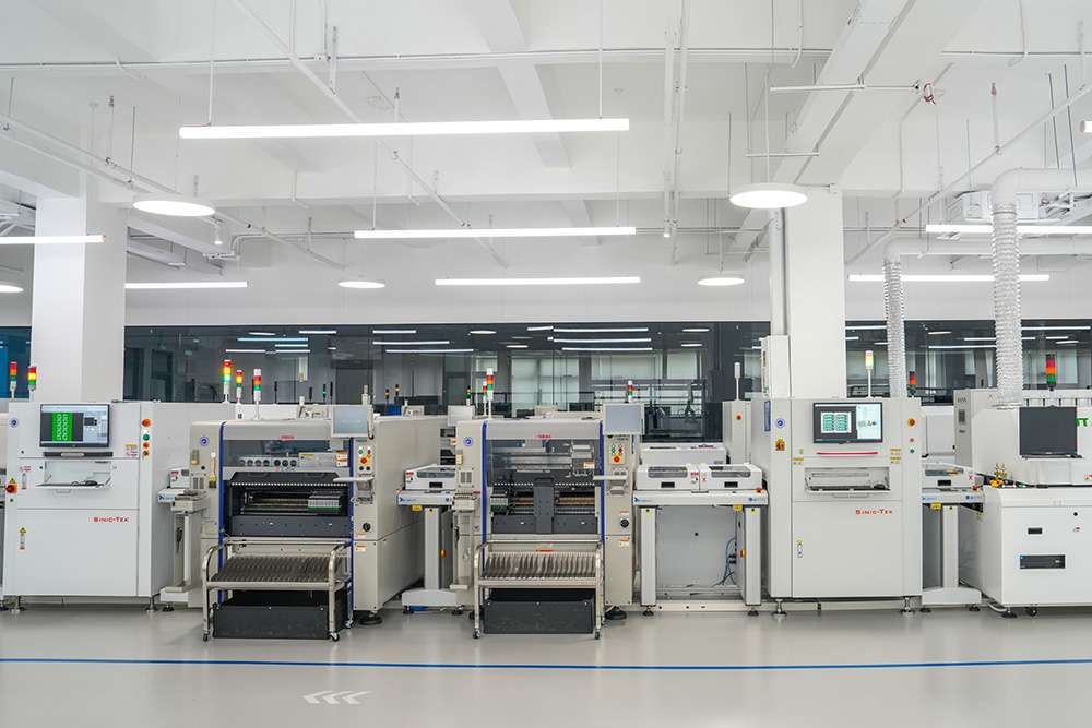


PCB Assembly Manufacturer Capabilities
Items | Information |
|---|---|
PCB Board Type | Rigid PCB, Rigid-FlexPCB, FlexPCB |
PCB Board Thickness | 0.1mm(min), 10mm(max) |
PCB Panel Size | 50mm*50mm(min), 810mm*610mm(max) |
SMT Component Size Range | 01005(min), 55mm*100mm*28mm(max) |
SMT Component Pitch Range | ≥0.35mm |
SMT Repeat Accuracy | ±0.025mm |
DIP Component Size Range | Height of component<120mm |
Protective N2 Gas Purity Of SMT&DIP | 99.999% |
SMT Assembly Manufacturer Process

IQC
IQC in PCBA inspects incoming components and materials for defects, compliance, and functionality before assembly. It prevents defects, reduces rework, and ensures reliability by verifying specs, dimensions, and electrical performance.

PCB cleaning
Before applying solder paste, PCBs must be thoroughly cleaned to ensure optimal stencil printing and soldering quality. Contaminants like dust, oils, oxidation, or residual flux can cause poor paste adhesion, misprints, or soldering defects.

Solder paste printer
A solder paste printer is a critical PCB Assembly machine that accurately deposits solder paste onto PCB pads before component placement. It ensures precise, consistent application for strong electrical connections during reflow soldering.

3D-SPI
3D-SPI is an advanced inspection system in PCBA to verify the quality, volume, and alignment of solder paste deposits after printing but before component placement. It ensures defect-free soldering and prevents reflow issues

Mounting Machine
Mounting (or component placement) is the process of accurately positioning and attaching electronic components onto a PCB after solder paste application. Mounting is a foundational step in PCBA, directly impacting soldering quality and final product reliability

FAI
FAI (First Article Inspection) is a critical quality control process performed on the first batch of assembled PCBs to verify that the manufacturing process meets design specifications before full-scale production.

2D-AOI
2D-AOI (Automated Optical Inspection) before reflow is a critical quality checkpoint in the SMT assembly process. It inspects the PCB after solder paste printing and component placement, but before the board enters the reflow oven.

Ersa reflow oven
Reflow oven can melt solder paste to permanently attach components to a PCB. It applies controlled heat to follow a precise temperature profile, ensuring reliable solder joints without damaging components.

3D-AOI
3D-AOI (3D Automated Optical Inspection) is a post-reflow inspection system that uses structured light, lasers, or multi-angle cameras to scan solder joints and components in three dimensions, detecting defects that 2D-AOI might miss.

X-ray
An X-ray inspection machine is a non-destructive testing (NDT) system used to examine hidden solder joints, internal PCB layers, and complex components that optical inspection cannot detect.
DIP Assembly Manufacturer Process

Preprocessing
DIP preprocessing steps: Capture → Denoise (median/NLM) → Enhance (CLAHE) → Detect edges (Canny) → Segment (Otsu) → Analyze defects. Optimizes inspection of pins and solder joints.

Component insertion
DIP insertion aligns pins with PCB holes manually or automatically, ensuring proper seating and straight pins. Automated systems apply 1-5N/pin force; manual needs visual checks. Done after SMT to avoid thermal issues.

2D-AOI
2D-AOI inspection after DIP component insertion checks for proper placement, verifying all components are present, correctly oriented, and fully seated with straight pins, while detecting any physical defects or misalignments before soldering to ensure assembly quality.

Automatic wave soldering
Automatic wave soldering for DIP components applies flux, preheats the PCB, then passes it over a molten solder wave to form reliable through-hole connections, with conveyor speed and wave height tightly controlled to prevent bridging or cold joints.

Automatic selective wave soldering
Selective wave soldering targets through-hole parts with localized flux and mini-wave nozzles, protecting nearby SMT components. This efficient process minimizes waste and ensures reliable DIP connections on mixed-technology boards.

Cleaning machine
Cleaning machine removes flux residues and contaminants to ensure reliability after wave soldering, and prevents long-term corrosion and electrical failures in DIP assemblies.

Press-fit
Press-fit DIP components create solderless connections via interference fit, ideal for harsh environments. The compliant pins form gas-tight joints through elastic deformation, requiring precise PCB holes but eliminating thermal soldering stress.

2D-AOI
2D-AOI after wave soldering checks DIP solder joints for defects. It identifies bridges, insufficient/excess solder, and poor wetting using top-down imaging with diffused lighting. This automated inspection catches critical soldering issues before electrical testing.

De-paneling
Separates individual boards from production panels after DIP assembly. V-Scoring/Punching for simple breakaway designs. Router cutting for precise, dust-free separation. Laser Cutting for high-precision for fragile boards.

QA
As part of our PCB assembly services, QA is conducted to detect micro-level defects in solder joints and fine-pitch components, such as micro cracks, solder bridging, and insufficient solder. This detailed examination ensures high-quality, reliability, and compliance with strict industry standards for every PCB assembly we deliver.
PCBA Service - FAQ
That’s a great question, because most issues in a pcb assembly service actually happen at the NPI stage. What we usually do is start with a DFM and DFA review within 24 to 48 hours, so we can flag anything that might affect manufacturability early on. Then we suggest a small pilot build to validate real production conditions—things like stencil design, placement accuracy, and reflow profiles. Once everything is confirmed, we lock those parameters, which makes your transition into volume PCBA much smoother and far more predictable.
If you already have files ready, we’re happy to review them and share quick feedback.
We understand the concern—every pcb assembly manufacturer talks about quality, but what really matters is measurable results. In our smt assembly service, we typically maintain a first pass yield above 98.5% for stable products, and keep SMT defect rates below 500 DPPM. For more complex components like BGA, we control void rates within industry standards. More importantly, these numbers aren’t one-time results—they’re monitored continuously, so your pcb assembly service stays consistent over time.
If you have specific quality targets, we can align with them upfront.
That’s actually a very common pain point in pcb assembly. What makes the difference is whether the supplier treats production as repeatable engineering, not just execution. After NPI, we lock all key process parameters and maintain strict version control on SMT programs and documentation. We also run statistical process control in our smt assembly service, typically keeping CPK at or above 1.33 for critical steps. Combined with full traceability, this allows us to reproduce the same results across different batches—not just once, but long term.
Supply chain issues are something we deal with every day in global pcb assembly service. We work with authorized distributors and multiple sourcing channels, so we can react quickly when shortages happen. If needed, our engineering team can suggest alternative components that meet both performance and compliance requirements. For ongoing projects, we can also help set up buffer stock strategies to stabilize supply. The goal is to make sure your pcb assembly doesn’t get delayed because of sourcing uncertainty.
We know communication can make or break an overseas pcb assembly service experience. That’s why every project has a dedicated English-speaking project manager who stays with you from start to finish. You’ll receive regular updates, and we can share detailed inspection data like AOI or X-ray results when needed. Most technical questions are answered within 24 hours, often faster. Our goal is to make working with a remote pcb assembly manufacturer feel just as smooth as working with a local partner.
Yes, and we understand that for many customers, this isn’t optional. Our pcb assembly processes follow IPC-A-610 Class II or Class III standards depending on your application, and we operate under ISO 9001 quality systems. We also ensure compliance with RoHS and REACH requirements. If your project involves stricter industries like automotive or medical, we can apply additional controls within the pcb assembly service to meet those expectations.
That’s exactly the right mindset. In our experience, the lowest unit price rarely means the lowest overall cost. A well-managed pcb assembly service focuses on total cost of ownership—things like reducing rework, avoiding delays, and preventing field failures. By improving first-pass yield and optimizing processes in our smt assembly service, we help you save costs where it really matters, without compromising reliability.
If you’d like, we can review your design and suggest cost optimization points.
Absolutely, and that’s something we plan for from the beginning. Our pcb assembly manufacturer capabilities are built to support the full lifecycle—from prototype to mass production. Once your process is validated, scaling is mainly about capacity, not re-learning. With multiple SMT lines and production planning aligned to forecasts, we can increase volume while keeping the same quality standards. That way, your pcb assembly service stays stable even as your business grows.
Inquire About PCB Assembly Services
sales@melinegroup.com
sales@melinegroup.net
Phone Number
+(86) 755 2732 7599
+(86) 755 2732 7699
Shenzhen (Headquarters)
Buildings 2 & 4, Fuqiao 4th Industrial Zone, Fuhai Street, Bao'an District, Shenzhen, Guangdong, China.
Chengdu
Room 905, Kailong Metropolitan Building, Chenghua District, Chengdu, China.
Chongqing
21-4A, Building 3, Daya Jinkai International, Yubei District, Chongqing, China.
Ontario
3281 E.Guasti Rd., Suite 270, Ontario, CA 91761,USA
Jiangxi
JinshanTown, Shangli County, Pingxiang City, Jiangxi, China