
Expert PCB Fabrication & Manufacturing Solutions
Precision Bare PCB Manufacturing for reliable electronics.
PCB Fabrication Services
Meline Group delivers professional PCB fabrication services, part of our comprehensive electronics manufacturing services (EMS), in full compliance with international quality and safety standards. Certified to ISO 9001, UL (E466113 for US and Canada), TS 16949, and RoHS, we provide reliable printed circuit board fabrication and bare PCB manufacturing for industrial, automotive, and high-reliability applications. Supported by a stable supply chain and strong manufacturing partnerships, our PCB manufacturing capabilities cover 2–60 layer PCBs, including HDI, high-frequency boards, backplanes, heavy copper, metal-based, flexible, and rigid-flex designs—ensuring consistent quality, controlled lead times, competitive pricing, and dependable after-sales support.

Benefits of Working with Meline Group
We deliver complete PCB fabrication services from double-sided boards to high-density, high-layer-count multilayer PCBs, ensuring smooth transitions from rapid prototyping to stable volume production.
We fabricate a full range of PCBs, including aluminum PCBs, flex PCBs, and other circuit board types, with strict process control and meticulous attention to detail to ensure consistent quality on every order.
We support a wide range of PCB materials, including FR4, high-Tg FR4, Rogers, metal-based, and high-frequency laminates, enabling reliable PCB fabrication tailored to diverse application requirements.
PCB Fabrication Capacities
Items | Information |
|---|---|
PCB Type | ICS, Backplane, HDI, High multi layer blind&buried PCB, Ceramic, Metal Base, Rigid-f lex PCB, Flex PCB |
Surface Finish | Flash gold, ENIG, Hard gold, HASL, LF-HASL, OSP, ENEPIG, Soft gold, Immersion silver, |
Special Process | Backdrill, Via in pad, Countersink, Depth control drilling, Peelable Mask, Carbon Ink |
Max PCB Size | Multi layer:1244*570mm, Double layer:1500*650mm |
Technical ability | Min.Hole Size: 0.1mm; Min.trace width: 0.05mm; Copper Thickness: H OZ-20 OZ; |
Raw Material Brand | Shengyi, ITEQ, KB, Panasonic, Isola, Rogers series, DuPont, Taconic, Arlon, Mitsubish, Hitachi |
Main supplier | SCC, Suntak, Fastprint, Sunshine |
Bare PCB Manufacturing Process
1. Pre-production Engineering
Pre-production engineering in PCB fabrication ensures bare PCB manufacturing readiness through manufacturing data review and early DFM optimization. Fabrication risks related to trace geometry, vias, spacing, and stack-up are identified and corrected, while signal, power, and thermal performance are evaluated to control impedance, reduce EMI, and improve reliability. Material selections—including FR-4, high-Tg FR-4, and Rogers laminates—along with copper thickness, solder mask, and surface finish options such as ENIG, HASL, and OSP are verified to ensure compatibility with fabrication requirements and stable production.

2. Inner Layer Imaging
Inner layer imaging transfers circuit patterns onto copper-clad inner layers by exposing photoresist-coated copper to UV light through precision photomasks, hardening the resist only where conductive traces are required. After development, chemical etching removes unprotected copper, and the remaining photoresist is stripped away, leaving the intended copper circuitry. Automated Optical Inspection (AOI) compares the imaged patterns against design data to detect defects such as opens, shorts, and line width deviations. This process ensures inner layer circuit accuracy and integrity before multilayer lamination, providing a stable foundation for subsequent PCB fabrication steps.

3. Lamination
Lamination forms the multilayer PCB structure by bonding inner circuit layers into a single solid board. Before lay-up, inner layer copper surfaces undergo oxide or alternative surface treatment to microscopically roughen the copper and enhance interlayer adhesion. During stack-up, inner cores, prepreg materials, and outer copper foils are precisely aligned according to the approved layer configuration. Under controlled heat and pressure, the prepreg resin flows and cures, fusing all layers into a void-free, mechanically stable structure. This process ensures strong interlayer bonding, stable dielectric properties, and long-term electrical and thermal reliability for high-density, high-layer-count PCB fabrication.

4. Drilling
Drilling creates vias and through-holes that electrically interconnect PCB layers and support subsequent metallization. X-ray drilling is used to locate inner layer targets and create precise tooling holes, ensuring accurate multilayer registration. High-speed CNC mechanical drilling with micro carbide bits then forms vias and plated through-holes across a wide diameter range, maintaining positional accuracy and clean hole walls. Tight control of spindle speed, feed rate, and drilling depth minimizes smear and mechanical stress, ensuring reliable copper plating and long-term interlayer connectivity. Precision drilling is essential to PCB performance, signal integrity, and structural reliability in multilayer and high-density PCB fabrication.

5. Electroless & Electrolytic Copper Plating
After drilling, desmear and copper plating processes establish reliable interlayer electrical connections. Desmear removes epoxy residue and glass fiber debris from hole walls, exposing clean copper surfaces for metallization. Electroless copper plating then deposits a thin, uniform conductive layer inside vias and through-holes. This is followed by electrolytic copper panel plating, which increases copper thickness across the panel surface and within holes. Controlled plating ensures uniform copper distribution, strong adhesion, and low electrical resistance, providing a stable foundation for outer layer imaging and long-term PCB reliability.
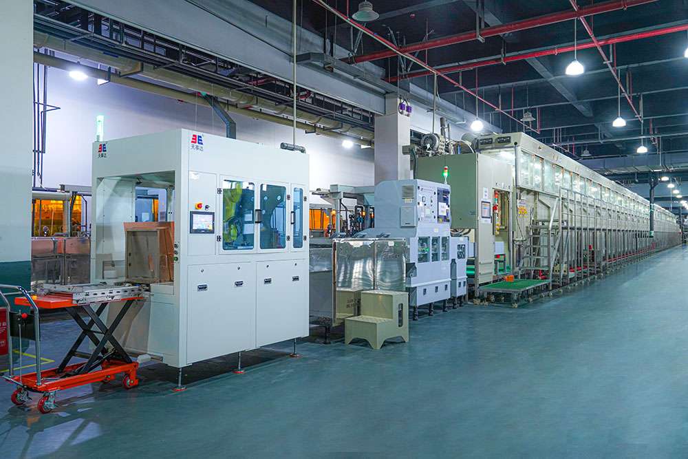
6. Outer Layer Imaging
The outer layer process defines the final circuit patterns on the PCB surface. Circuit images are transferred to photoresist-coated copper using precise UV exposure, followed by developing to remove unexposed resist and reveal trace areas. Pattern plating then electroplates copper to build conductor thickness, with tin applied as an etch-resistant layer. The strip-etch-strip process removes remaining photoresist, etches excess copper, and strips the protective tin, leaving accurate outer layer circuits. Automated Optical Inspection (AOI) verifies trace width, spacing, and circuit continuity, ensuring impedance control, dimensional accuracy, and long-term reliability prior to surface finishing.
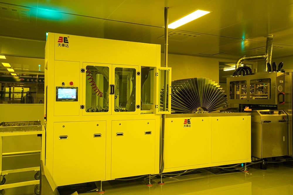
7. Solder Mask Application
Solder mask application protects exposed copper and defines solderable areas on the PCB. Via holes are first treated using plasma or chemical processes to clean and prepare the surfaces for optimal solder mask adhesion. Liquid photoimageable (LPI) solder mask is then applied and partially cured to achieve a tack-free surface. UV exposure through a photomask hardens the solder mask in designated areas, followed by developing to remove unexposed material and accurately open pads and vias. A final thermal cure fully polymerizes the solder mask, ensuring long-term durability, electrical insulation, and resistance to environmental and mechanical stress.
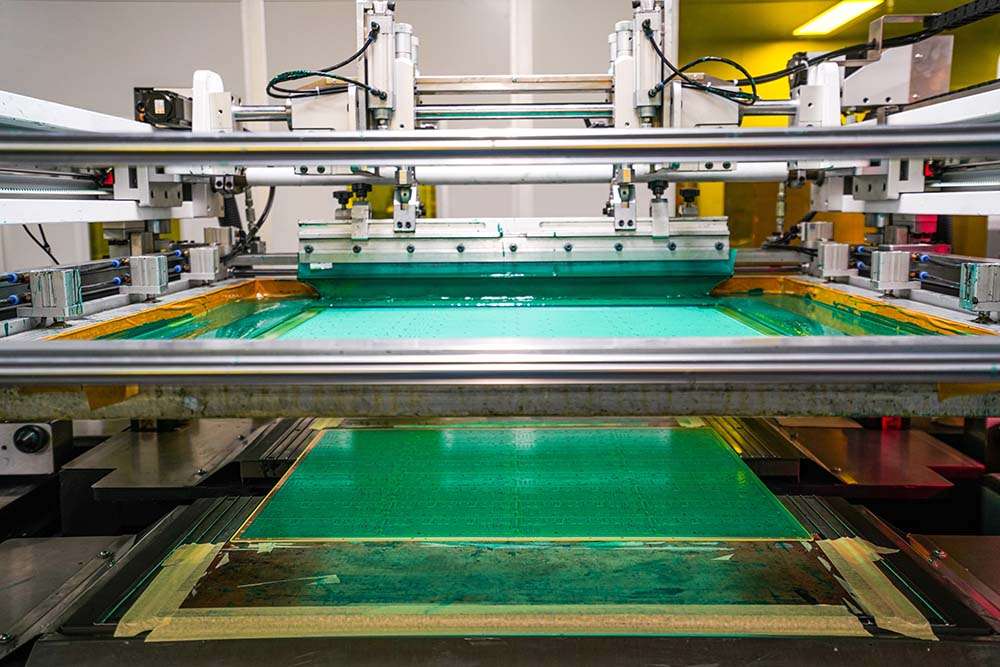
8. Silkscreen / Legend Printing
Legend printing applies permanent component identifiers, reference designators, and markings to the PCB surface. Epoxy-based inks are applied using inkjet or traditional screen-printing methods to ensure clear and accurate legends. A controlled pre-drying stage at low temperature removes residual solvents and prevents ink smearing or distortion. Final high-temperature curing fully hardens the ink, providing strong adhesion to the solder mask and resistance to abrasion, chemicals, and environmental exposure. This process ensures long-lasting readability and accurate assembly guidance while supporting product identification and branding requirements.

9. Surface Finish
Surface finishing protects exposed copper pads and ensures reliable solderability during assembly. ENIG (Electroless Nickel Immersion Gold) provides a flat, durable surface with excellent oxidation resistance, making it suitable for fine-pitch and high-reliability applications. Immersion tin offers good solderability and planarity but has a relatively shorter shelf life. HASL (Hot Air Solder Leveling) coats pads with solder, delivering a cost-effective and robust finish, though with less surface flatness. The selected surface finish balances cost, solderability, shelf life, and planarity based on application requirements.

10. Profiling (Rout & V-Scoring)
Profiling defines the final board outline and panel separation method. V-scoring uses angled blades to create controlled grooves along straight lines, leaving a thin web that allows easy and low-cost separation, making it ideal for simple, rectangular panel designs. CNC routing precisely mills board contours, enabling complex shapes, curves, slots, and internal cutouts with high dimensional accuracy. In practical production, routing and V-scoring are often combined—V-scoring for efficient panel separation and routing for complex features—ensuring manufacturing efficiency while meeting mechanical and assembly requirements.

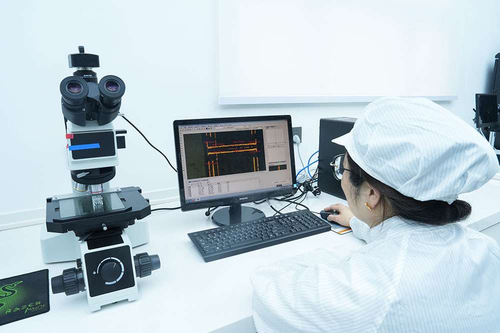
11. Inspection & Testing
Inspection and testing verify that finished PCBs meet electrical, mechanical, and quality requirements. Electrical testing is performed using flying probe systems or dedicated test fixtures to detect shorts, opens, and netlist errors, with impedance testing applied where high-speed performance is specified. Final inspection combines visual examination and Automated Optical Inspection (AOI) to identify surface defects in solder mask, silkscreen, and copper features. Dimensional checks confirm board thickness, hole diameters, and outline accuracy. Final quality control includes AQL-based sampling audits in accordance with IPC Class 2 or Class 3 standards, ensuring consistent quality prior to packaging and shipment.
12. Packaging
Packaging protects finished PCBs during storage and transportation while maintaining production readiness. Boards are first cleaned to remove debris and ionic contaminants, followed by anti-tarnish treatment when required to protect exposed finishes. Moisture-sensitive PCBs are vacuum-sealed with desiccants and moisture barrier materials, while ESD-sensitive products are packed in static-shielding bags. Sturdy outer packaging with proper cushioning prevents mechanical damage during transit. Clear labeling, including barcodes, handling instructions, and compliance markings, ensures traceability, safe handling, and efficient logistics upon delivery.
PCB Types We Fabricate
Basic PCBs – Pfofessional Solutions for Standard Applications
Rigid PCB – Standard multi-layer PCBs for general electronics, offering stable electrical performance and reliable manufacturability.
Flexible PCB – Lightweight, bendable PCBs ideal for compact devices, wearables, and applications requiring dynamic flexibility.
HDI PCB – High-Density Interconnect PCBs with finer traces and smaller vias, perfect for compact, high-performance designs.
Aluminum PCB – Metal-core PCBs optimized for heat dissipation in LED lighting, power modules, and industrial electronics.
Moderate PCBs – Advanced Performance for Specialized Needs
High-Speed PCB – Engineered for high-frequency digital signals, maintaining signal integrity in fast computing, telecom, and networking devices.
High-Frequency PCB – Designed for RF/microwave applications, minimizing dielectric loss for wireless, radar, and 5G systems.
Metal Core PCB – Optimized for thermal management in power electronics and LED applications, combining conductivity and heat dissipation.
Rigid-Flex PCB – Combines rigid and flexible layers for compact, dynamic designs in medical devices, aerospace, and industrial electronics.
Advanced PCBs – Cutting-Edge Technology for High-Precision Applications
IC Substrate – High-precision interposers for semiconductor packaging, ensuring reliable connections for advanced ICs.
Ceramic PCB – Superior thermal conductivity and stability for aerospace, automotive, and high-reliability electronics.
Glass Substrate PCB – Ultra-high-frequency applications requiring minimal signal loss, used in advanced communication and sensor systems.
Ceramic-Polymer Hybrid PCB – High-performance ceramic-polymer for reliable aerospace, automotive, and industrial electronics.
FAQs about Our PCB Fabrication Services
When selecting a PCB fabrication supplier, procurement should assess risks related to lamination control, drilling accuracy, copper plating uniformity, and material traceability. Inadequate process control may result in impedance deviation, weak interlayer bonding, or inconsistent quality between batches—leading to yield loss, requalification costs, and supply instability.
PCB fabrication quality directly impacts signal integrity, thermal performance, and mechanical stability. Poor copper uniformity, inaccurate drilling, or weak interlayer bonding can lead to impedance deviation, delamination, or early field failures, especially in high-density and high-speed designs.
Process stability is maintained through technology-specific fabrication controls tailored to different PCB types, layer counts, and stack-up structures. Key parameters such as lamination profiles, drilling tolerances, copper plating thickness, and etching compensation are adjusted based on material systems, aspect ratios, and impedance requirements. Standardized process windows, in-process inspections, and batch traceability ensure consistent electrical and mechanical performance across single-layer, multilayer, HDI, and high-reliability bare PCB fabrication.
Common PCB fabrication materials include FR-4, high-Tg laminates, RF materials such as Rogers, metal-core substrates, and polyimide for flexible circuits. Material selection depends on operating temperature, frequency performance, dielectric stability, and reliability requirements.
Professional PCB fabrication typically supports 2 to 60 layers, depending on design complexity and manufacturing requirements. High-layer-count PCBs require precise registration, controlled lamination cycles, and stable dielectric thickness to ensure electrical consistency.
PCB manufacturing operations are governed by a combination of internationally recognized quality systems and process control standards. Manufacturing workflows are typically aligned with ISO 9001–based quality management systems, while production and inspection criteria follow IPC specifications such as IPC-6012 for rigid printed boards and IPC-A-600 for visual acceptance. For high-reliability applications, enhanced process controls, traceability, and inspection levels are implemented to meet stricter customer and industry requirements. These standards ensure consistent build quality, controlled manufacturing variation, and long-term electrical and mechanical reliability across bare PCB production.
Process consistency in PCB fabrication is achieved through standardized process parameters, controlled material sourcing, documented work instructions, in-process inspections, and traceability from raw materials to finished bare PCBs. Manufacturers lacking batch-level control often show large quality variation between pilot and volume production.
To initiate PCB fabrication, manufacturers typically require Gerber files, drill data, approved stack-up details, material specifications, impedance requirements, and fabrication notes. Clear documentation helps ensure the fabricated PCB accurately matches the design intent.
Surface finish selection impacts not only solderability but also shelf life, planarity, and assembly yield. Inconsistent surface finish control may cause oxidation, poor wetting, or coplanarity issues during PCB assembly. Reliable PCB fabrication suppliers verify finish compatibility with customer assembly processes and storage requirements before volume production.
After fabrication, bare PCBs are cleaned, protected against oxidation if required, vacuum-sealed with moisture barriers and desiccant, packed in ESD-safe materials, and labeled for traceability to ensure they arrive assembly-ready.
Still have questions about your PCB manufacturing project?
Share your requirements and our engineering team will review them with you. ↓ ↓ ↓
Discuss Your PCB Manufacturing Requirements
sales@melinegroup.com
sales@melinegroup.net
Phone Number
+(86) 755 2732 7599
+(86) 755 2732 7699
Shenzhen (Headquarters)
Buildings 2 & 4, Fuqiao 4th Industrial Zone, Fuhai Street, Bao'an District, Shenzhen, Guangdong, China.
Chengdu
Room 905, Kailong Metropolitan Building, Chenghua District, Chengdu, China.
Chongqing
21-4A, Building 3, Daya Jinkai International, Yubei District, Chongqing, China.
Ontario
3281 E.Guasti Rd., Suite 270, Ontario, CA 91761,USA
Jiangxi
JinshanTown, Shangli County, Pingxiang City, Jiangxi, China